

The Most Complex 2D Microchip Yet
Scientists hope that two-dimensional materials such as graphene or molybdenum disulfide will allow Moore’s Law to continue apace once it becomes impossible to make further progress using silicon. A 3-atom-thick microchip developed by researchers at the Vienna University of Technology (VUT) may be the first example of 2D materials following the seemingly inexorable growth in the number of transistors in integrated circuits that Gordon Moore observed decades ago.
Previously, the number of transistors on ICs made from 2D materials had remained in the single digits, says study senior author Thomas Müller, an electrical engineer at VUT. The chip that he and his colleagues created boasts 115 transistors. They described their device on 11 April in the journal Nature.
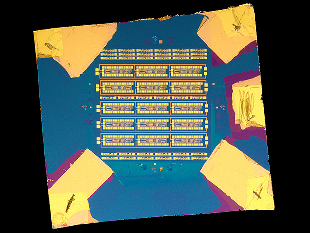
Photo: Stefan Wachter
Flat and Packed: The prototype processor consumes about 60 microwatts and contains 115 transistors. Its designers hope to integrate more.
The microchip can execute user-defined programs stored in external memory, perform logic operations, and transmit data to its periphery. Although this prototype operates on single-bit data, the researchers say their design is readily scalable to multibit data. They also note their invention is compatible with existing semiconductor manufacturing processes.
The new device is made of a thin film of molybdenum disulfide, which resembles a sheet of molybdenum atoms sandwiched between two layers of sulfur atoms. The film is only six-tenths of a nanometer thick. In comparison, the active layer of a silicon microchip can be up to about 100 nanometers thick.
“It’s exciting that the authors have been able to build circuits of this complexity using an atomically thin 2D material that has only been studied for five years,” says Eric Pop, an electrical engineer at Stanford University, who did not take part in this research.
So, what’s molybdenum disulfide’s Moore’s Law potential? The minimum size of features in the VUT prototype was a rather chunky 2 micrometers. However, “Going to 200- or 100-nanometer transistor channel lengths should be rather straightforward,” says Müller. He adds that improvements in the quality of electrical contacts in these circuits should result in an ultimate scaling limit for 2D transistors of about 1 nanometer. “This cannot be reached with silicon; the limit there is around 5 nanometers,” says Müller.
The main obstacle to building even more complex microchips with molybdenum disulfide is the trouble the team has had with fabricating transistors. Currently, Müller’s team’s yield for fully functional chips is only a few percent. One way to increase transistor yield is to grow more-uniform molybdenum disulfide films, he says. Unfortunately, imperfections in the films crop up when they are transferred from the sapphire substrates on which they are grown to their target wafers, he explains. The researchers are now working on ways to grow the molybdenum disulfide film directly on the target wafer to remove this transfer step. By improving the uniformity of molybdenum disulfide films, “it should be rather straightforward to increase the complexity of two-dimensional circuits to tens of thousands of transistors,” Müller says.
No Comments